- 您现在的位置:买卖IC网 > Sheet目录540 > ZXMN3A03E6TC (Diodes Inc)MOSFET N-CHAN 30V SOT23-6
ZXMN3A03E6
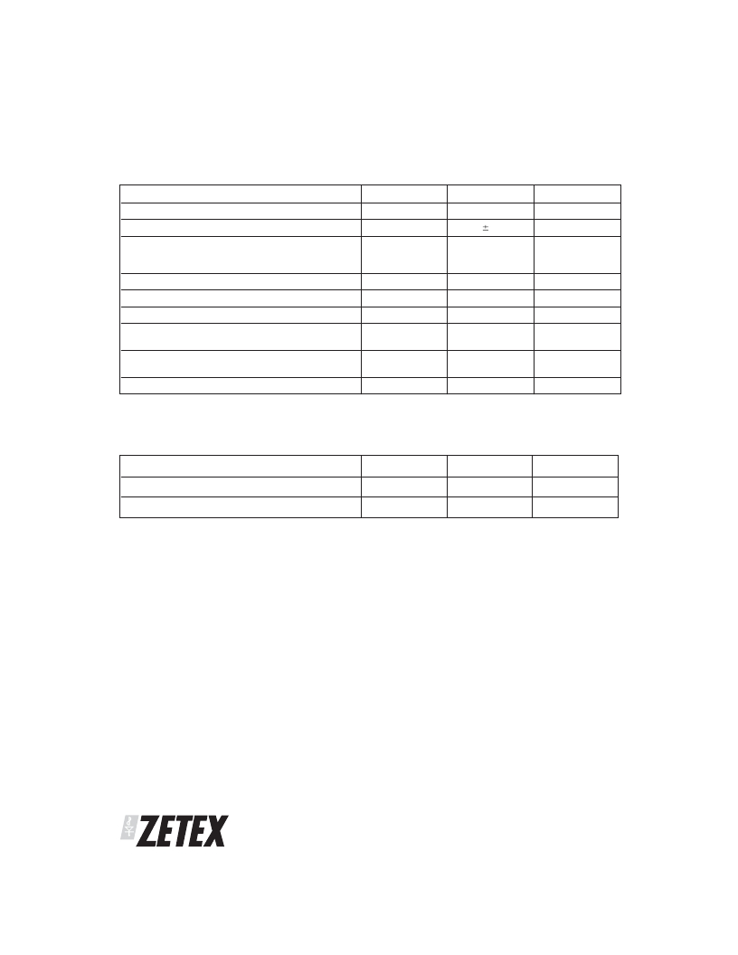
ABSOLUTE MAXIMUM RATINGS.
PARAMETER
Drain-source voltage
Gate source voltage
Continuous drain current V GS =10V; T A =25°C (b)
V GS =10V; T A =70°C (b)
V GS =10V; T A =25°C (a)
Pulsed drain current (c)
SYMBOL
V DSS
V GS
I D
I DM
LIMIT
30
20
4.6
3.7
3.7
17
UNIT
V
V
A
A
Continuous source current (body diode)
Pulsed source current (body diode) (c)
(b)
I S
I SM
2.6
17
A
A
Power dissipation at T A =25°C
Linear derating factor
(a)
P D
1.1
8.8
W
mW/°C
Power dissipation at T A =25°C (b)
Linear derating factor
Operating and storage temperature range
P D
T j :T stg
1.7
13.6
-55 to +150
W
mW/°C
°C
THERMAL RESISTANCE
PARAMETER
SYMBOL
VALUE
UNIT
Junction to ambient
Junction to ambient
(a)
(b)
R θ JA
R θ JA
113
73
°C/W
°C/W
NOTES:
(a) For a device surface mounted on 25mm x 25mm FR4 PCB with high coverage of single sided 1oz copper, in still air conditions
(b) For a device surface mounted on FR4 PCB measured at t 10 secs.
(c) Repetitive rating 25mm x 25mm FR4 PCB, D = 0.05, pulse width 10 s - pulse width limited by maximum junction temperature. Refer to
Transient Thermal Impedance graph.
ISSUE 3 - OCTOBER 2005
SEMICONDUCTORS
2
发布紧急采购,3分钟左右您将得到回复。
相关PDF资料
ZXMN3A04DN8TC
MOSFET DUAL N-CHAN 30V 8SOIC
ZXMN3A04KTC
MOSFET N-CH 30V 18.4A DPAK
ZXMN3A06DN8TC
MOSFET DUAL N-CHAN 30V 8SOIC
ZXMN3A14FTA
MOSFET N-CH 30V 3.2A SOT23-3
ZXMN3AM832TA
MOSFET N-CHAN DUAL 30V 8MLP
ZXMN3AMCTA
MOSFET 2N-CH 30V 2.9A DFN
ZXMN3B01FTA
MOSFET N-CHAN 30V 2A SOT23-3
ZXMN3B04N8TC
MOSFET N-CHAN 30V 8SOIC
相关代理商/技术参数
ZXMN3A04DN8
制造商:Diodes Incorporated 功能描述:MOSFET DUAL N SO-8
ZXMN3A04DN8
制造商:Diodes Incorporated 功能描述:MOSFET N DUAL SO-8
ZXMN3A04DN8_02
制造商:ZETEX 制造商全称:ZETEX 功能描述:DUAL 30V N-CHANNEL ENHANCEMENT MODE MOSFET
ZXMN3A04DN8TA
功能描述:MOSFET Dl 30V N-Chnl UMOS RoHS:否 制造商:STMicroelectronics 晶体管极性:N-Channel 汲极/源极击穿电压:650 V 闸/源击穿电压:25 V 漏极连续电流:130 A 电阻汲极/源极 RDS(导通):0.014 Ohms 配置:Single 最大工作温度: 安装风格:Through Hole 封装 / 箱体:Max247 封装:Tube
ZXMN3A04DN8TC
功能描述:MOSFET Dl 30V N Chnl UMOS RoHS:否 制造商:STMicroelectronics 晶体管极性:N-Channel 汲极/源极击穿电压:650 V 闸/源击穿电压:25 V 漏极连续电流:130 A 电阻汲极/源极 RDS(导通):0.014 Ohms 配置:Single 最大工作温度: 安装风格:Through Hole 封装 / 箱体:Max247 封装:Tube
ZXMN3A04K
制造商:ZETEX 制造商全称:ZETEX 功能描述:30V N-CHANNEL ENHANCEMENT MODE MOSFET IN DPAK
ZXMN3A04KTC
功能描述:MOSFET N-Ch 30 Volt 18.4A RoHS:否 制造商:STMicroelectronics 晶体管极性:N-Channel 汲极/源极击穿电压:650 V 闸/源击穿电压:25 V 漏极连续电流:130 A 电阻汲极/源极 RDS(导通):0.014 Ohms 配置:Single 最大工作温度: 安装风格:Through Hole 封装 / 箱体:Max247 封装:Tube
ZXMN3A05N8TA
功能描述:MOSFET N-CH 30V 12A 8-SOIC RoHS:否 类别:分离式半导体产品 >> FET - 单 系列:- 标准包装:1,000 系列:MESH OVERLAY™ FET 型:MOSFET N 通道,金属氧化物 FET 特点:逻辑电平门 漏极至源极电压(Vdss):200V 电流 - 连续漏极(Id) @ 25° C:18A 开态Rds(最大)@ Id, Vgs @ 25° C:180 毫欧 @ 9A,10V Id 时的 Vgs(th)(最大):4V @ 250µA 闸电荷(Qg) @ Vgs:72nC @ 10V 输入电容 (Ciss) @ Vds:1560pF @ 25V 功率 - 最大:40W 安装类型:通孔 封装/外壳:TO-220-3 整包 供应商设备封装:TO-220FP 包装:管件
